Introduction
Hexagonal boron nitride (h-BN) ceramics are increasingly used in high-temperature, high-purity, and electrically sensitive manufacturing environments. Owing to their unique combination of thermal stability, electrical insulation, chemical inertness, and excellent machinability, h-BN ceramics have become essential materials in photovoltaic silicon production and semiconductor manufacturing equipment.
This article provides a technical overview of h-BN ceramic materials, focusing on their intrinsic material properties and practical applications in industrial environments where conventional oxide ceramics or graphite components reach their performance limits.
1. Overview of Hexagonal Boron Nitride Ceramics
Hexagonal boron nitride is a non-oxide ceramic composed of boron and nitrogen atoms arranged in a layered hexagonal crystal structure. This structure is often compared to graphite due to its lamellar nature; however, unlike graphite, h-BN is electrically insulating and chemically more inert.
Industrial-grade h-BN ceramics are typically produced with purity levels exceeding 99.5%, ensuring minimal contamination risk in high-temperature and high-purity processes. The material remains stable up to 2800 °C in vacuum environments and can operate continuously at approximately 1000 °C in air, making it suitable for demanding thermal processes.
2. Key Material Properties of h-BN Ceramics
2.1 High-Temperature Stability
h-BN ceramics exhibit exceptional thermal resistance:
- Maximum service temperature in vacuum: up to 2800 °C
- Continuous operation temperature in air: ~1000 °C
This thermal stability allows h-BN components to function reliably in crystal growth furnaces, vacuum chambers, and high-temperature processing equipment.
2.2 Electrical Insulation
One of the most distinctive features of h-BN ceramics is their excellent electrical insulation, with a volume resistivity exceeding 10¹⁴ Ω·cm.
This property is particularly critical in semiconductor and photovoltaic equipment, where electrical isolation must be maintained at elevated temperatures.
2.3 Thermal Conductivity and Thermal Shock Resistance
h-BN ceramics combine moderate-to-high thermal conductivity (30–40 W/m·K) with a low coefficient of thermal expansion. This combination enables:
- Efficient heat dissipation
- Reduced thermal stress
- Strong resistance to thermal shock during rapid heating and cooling cycles
Such behavior is uncommon among electrically insulating ceramics and provides a significant advantage in thermally dynamic processes.
2.4 Chemical Inertness and Non-Wetting Behavior
Hexagonal boron nitride is chemically inert to most acids, alkalis, salts, and molten metals.
In addition, molten metals do not wet h-BN surfaces, preventing adhesion and contamination. This makes h-BN an ideal material for crucibles, evaporation boats, and containment components used in high-purity melting and deposition processes.
2.5 Low Friction and Machinability
The layered crystal structure of h-BN provides intrinsic lubricity, resulting in a low friction coefficient even under dry or high-temperature conditions.
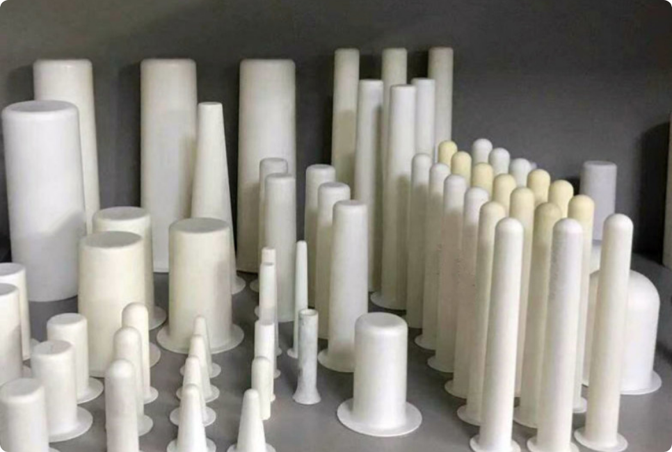
Compared with many advanced ceramics, h-BN has relatively low hardness, allowing conventional machining (turning, milling, drilling) with carbide tools. This enables the fabrication of complex, customized components.
3. Applications in Photovoltaic Silicon Manufacturing
3.1 Application Environment
In the production of monocrystalline and polycrystalline silicon, h-BN ceramic components are used throughout high-temperature processes such as crystal growth, pulling, and ingot casting. Their role is to provide:
- High-temperature electrical insulation
- Low contamination risk
- Stable mechanical support
3.2 Typical h-BN Components Used in PV Equipment
- Insulation and thermal barrier components
(electrode protection tubes, insulation plates, sealing rings, thermal shields) - Crucibles and containers
Used for holding molten silicon, ensuring purity and chemical stability - Structural support components
Including crucible holders and support frames that maintain stability at high temperatures - Nozzles and flow-control parts
Used during crystal growth to regulate material input and gas flow - Evaporation boats
Applied in thin-film deposition processes to ensure uniform material evaporation
4. Applications in Semiconductor Manufacturing
4.1 Crystal Growth and Epitaxial Processes
h-BN ceramics are widely used in the growth of compound semiconductors such as GaAs, GaP, and InP.
In technologies like MBE (Molecular Beam Epitaxy) and MOCVD, h-BN components serve as:
- Crucibles for source materials
- Substrate holders and heater supports
Their thermal stability and electrical insulation help maintain a controlled growth environment.
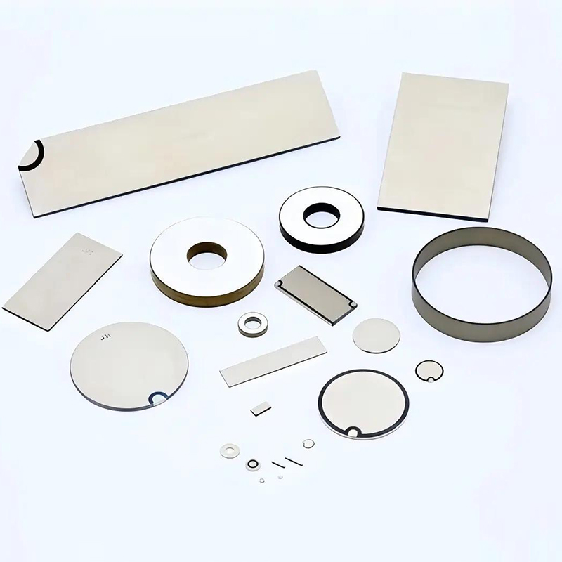
4.2 Semiconductor Equipment Components
In semiconductor fabrication equipment, h-BN ceramics are commonly used for:
- Wafer handling components
(robot arms, wafer clamps), where low friction and chemical inertness reduce wafer damage - Vacuum chamber components
Including insulating plates and seals that operate reliably under high vacuum and temperature - Heating elements and heaters
Such as heating tubes and plates, providing uniform heat distribution while preventing electrical breakdown
4.3 Packaging and Thermal Management
h-BN ceramics are also applied in:
- Thermally conductive insulating substrates
Used in semiconductor packaging to dissipate heat while maintaining electrical isolation - Heat dissipation components
Including heat sinks and thermal spreaders that help control device operating temperature
Conclusion
Hexagonal boron nitride ceramics offer a rare balance of high-temperature capability, electrical insulation, thermal conductivity, and chemical stability. These characteristics make h-BN an indispensable material in photovoltaic silicon manufacturing and semiconductor processing, where process stability and material purity are critical.
From crystal growth to wafer handling and thermal management, h-BN ceramics continue to replace conventional materials as process requirements become more demanding.