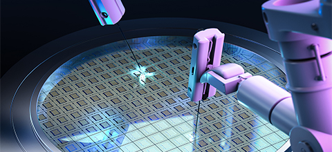
Introduction: Advanced Ceramics as the Silent Enablers of Semiconductor Manufacturing
In semiconductor manufacturing, material purity, thermal stability, and mechanical precision define process limits. Conventional metals and polymer-based materials can no longer withstand the increasingly extreme operating environments of modern semiconductor equipment, including ultra-high vacuum, elevated temperatures, high voltages, and aggressive plasma exposure.
As a result, advanced technical ceramics have become the silent foundation materials of the semiconductor industry. From wafer fabrication equipment and process chambers to packaging substrates and power electronic modules, ceramics now play a central role in enabling continuous technological scaling.
At Loongeram, advanced ceramics are engineered as reliability-critical system materials, not simply components. By aligning materials science with semiconductor manufacturing realities, Loongeram supports long-term process stability, yield protection, and equipment lifecycle extension.
1. Why Semiconductor Manufacturing Depends on Advanced Technical Ceramics
Every internal component of semiconductor fabrication equipment—wafer carriers, etching chambers, electrostatic chucks, thermal substrates, and insulating parts—operates under extreme physical and chemical conditions. Materials must remain stable under:
- Temperatures exceeding 1000 °C
- Continuous plasma and ion bombardment
- Ultra-high vacuum conditions
- High electric fields and power density
Limitations of Conventional Materials
- Metals offer good electrical and thermal conductivity but are prone to oxidation, sputtering, and contamination.
- Polymers lack the thermal and mechanical stability required for high-temperature processes.
Why Ceramics Are Different
Advanced ceramics provide a unique combination of properties essential to semiconductor manufacturing:
- Ultra-high purity and low contamination risk
Metal impurity levels can be controlled below 1 ppm, minimizing wafer surface contamination. - Exceptional thermal stability
Alumina and aluminum nitride remain dimensionally stable above 1000 °C. - High electrical insulation strength
Critical for electrostatic chucks (ESCs) and RF isolation components. - High hardness and wear resistance
Ideal for chamber liners, valve seats, and sliding seals. - Thermal expansion compatibility (CTE matching)
Enables reliable integration with silicon, GaN, and SiC, reducing thermal stress and cracking.
According to engineering evaluations referenced by Loongeram, replacing metal components with high-performance ceramics can extend equipment service life by 30–50%, while significantly reducing particle generation—directly supporting wafer yield improvement.
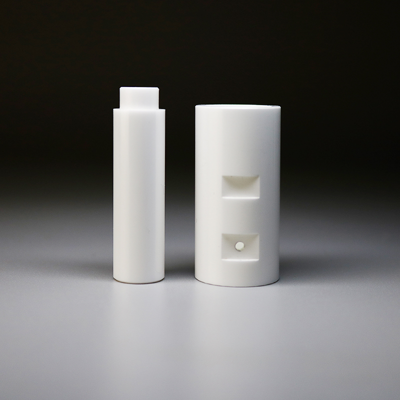
2. Key Ceramic Materials and Their Semiconductor Applications
| Ceramic Material | Core Properties | Typical Applications | Engineering Value |
|---|---|---|---|
| Alumina (Al₂O₃) | Electrical insulation, corrosion resistance, high strength | ESC bodies, insulation rings, support structures | Mature, cost-effective |
| Aluminum Nitride (AlN) | High thermal conductivity (>180 W/m·K), electrical insulation | Power module substrates, RF base plates | Thermal management benchmark |
| Silicon Nitride (Si₃N₄) | High strength, thermal shock resistance | Wafer carriers, load-bearing platforms | Metal replacement potential |
| Silicon Carbide (SiC) | Extreme hardness, plasma resistance, high thermal conductivity | Etching rings, chamber liners | Plasma-intensive environments |
| Zirconia (ZrO₂) | High fracture toughness, precision machinability | Alignment components, locating pins | Superior dimensional stability |
These materials are indispensable in both semiconductor fabrication equipment (SFE) and power electronics, where reliability directly impacts productivity and yield.
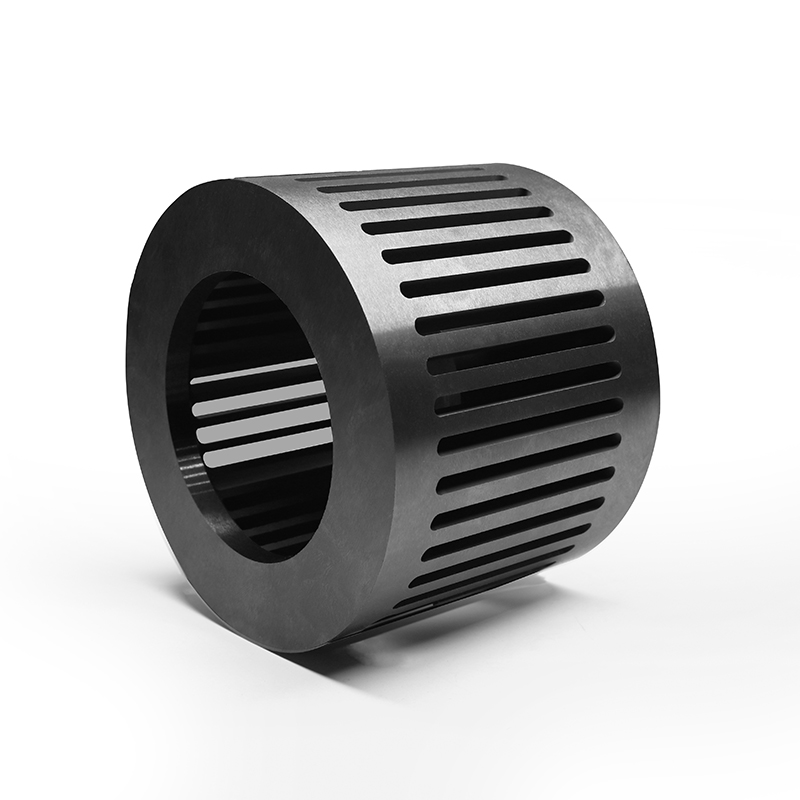
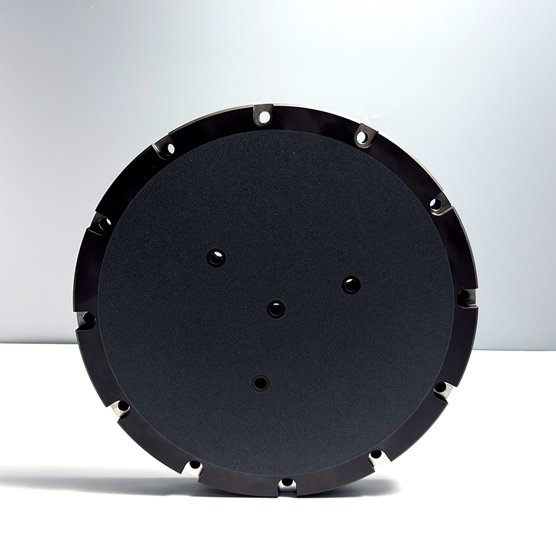
3. Applications in Wafer Fabrication Equipment
3.1 Electrostatic Chucks (ESCs)
Aluminum nitride–based ESCs are the industry standard due to their balanced thermal and electrical properties.
Key performance targets:
- Thermal conductivity ≥ 170 W/m·K
- Dielectric strength ≥ 10 kV/mm
- CTE matched to silicon (~4.5 × 10⁻⁶/K)
Loongeram focuses on oxygen-controlled AlN compositions and uniform microstructure design, ensuring stable thermal performance and electrical reliability under prolonged operation.
3.2 Etching Chambers and Reaction Liners
Dry etching processes using CF₄, Cl₂, and fluorine-based plasmas demand materials with extreme chemical inertness and erosion resistance.
- Reaction-bonded SiC (R-SiC)
- CVD SiC
have become mainstream solutions. High-purity SiC components can achieve service lifetimes exceeding 2000 hours, significantly outperforming conventional alumina parts.
3.3 Wafer Handling and Transport Components
Silicon nitride ceramics combine high mechanical strength with low density, making them ideal for:
- Wafer support arms
- Support rings
- Wafer trays
In rapid thermal processing (RTP) systems, Si₃N₄ components withstand repeated thermal cycling without cracking, improving tool uptime.
4. Applications in Power Electronics and Semiconductor Packaging
4.1 High-Power Module Substrates
The adoption of SiC and GaN power devices has significantly increased power density, making thermal management a critical bottleneck.
Ceramic substrates such as DBC (Direct Bonded Copper) and AMB (Active Metal Brazed) have become industry standards.
| Substrate Type | Ceramic Material | Thermal Conductivity (W/m·K) | Key Advantage |
|---|---|---|---|
| DBC-Al₂O₃ | Alumina | ~25 | Cost-effective |
| DBC-AlN | Aluminum nitride | ~180 | Superior heat dissipation |
| AMB-Si₃N₄ | Silicon nitride | ~90 | High toughness, thermal cycling resistance |
Loongeram emphasizes substrate-grade consistency, ensuring predictable thermal pathways and long-term module reliability.
4.2 Packaging Structures and Support Components
Alumina and zirconia ceramics are widely used for:
- Precision package housings
- Optoelectronic device bases
- MEMS package lids
Their stable dielectric properties and dimensional accuracy support high-frequency and high-reliability packaging designs.
5. Manufacturing Challenges and Reliability Control
Despite their advantages, advanced ceramics present significant manufacturing challenges:
- Sintering temperatures often exceed 1700 °C
- Tight dimensional control is required for semiconductor-grade components
With advances in CNC diamond machining, ultrasonic processing, and laser-assisted grinding, ceramic component tolerances can reach ±5 μm, meeting even EUV lithography equipment requirements.
At Loongeram, manufacturing control—from powder selection to final inspection—is treated as a reliability discipline, not merely a production step.
6. Future Trends: From Material Optimization to System-Level Engineering
As semiconductor technologies continue to evolve toward higher efficiency and smaller nodes, ceramic innovation is focusing on:
- Ultra-high-purity AlN ceramics
Oxygen content below 0.1 wt% for enhanced thermal conductivity. - Ceramic composite materials
ZrO₂- or Y₂O₃-reinforced Si₃N₄ for improved fracture toughness. - Ceramic–metal hybrid packaging
Combining low thermal resistance with high mechanical reliability, particularly for EV power modules. - Advanced manufacturing routes
Including ceramic 3D printing and reaction sintering for complex customized parts.
Conclusion: Materials Define the Future of Semiconductors
The pace of semiconductor innovation is ultimately constrained by material performance limits, and advanced technical ceramics represent one of the most critical enablers of future progress.From wafer fabrication to power electronics packaging, ceramics are no longer passive structural materials—they are active contributors to process stability, yield optimization, and system reliability.By integrating materials science expertise, manufacturing experience, and application-driven engineering, Loongeram positions advanced ceramics as a trusted foundation for next-generation semiconductor technologies.